By Dick Otte, CEO, Promex Industries
Cost and performance are the two most pressing issues in chip design and manufacturing. Chiplets are a key solution being pursued by the semiconductor industry to help mitigate these challenges. These small die with specialized functionality are designed to be combined to make up a larger device, following the industry trend of heterogeneous integration. In this post, we’re going to look at some of the challenges associated with assembling and packaging these complex devices – specifically, exploring optimizing chiplet packaging for complex applications.
With packaging technology poised to play a key role in the performance of next-generation systems, chiplets are emerging as one the most hotly pursued solutions. Chiplet-based designs can use a wide range of materials, and this single-package integration allows efficient integration of multiple silicon die using high density substrates, silicon interposers, bridges and other interconnect methods.
The rise of the chiplet era yielded creation in 2018 of the Open Compute Project’s (OCP) Open Domain-Specific Architecture (ODSA) subproject, which is focused on defining and developing a chiplet-based architecture and die-to-die interfaces. Built to address die disaggregation and IP reuse, ODSA supports efforts to advance an open chiplet ecosystem. Its charter includes addressing design and industry collaboration challenges, as well as staying on top of such questions as:
- What chiplets are available – details, datasheets, other information
- Vendors/sources for interposers – capabilities, delivery times, pricing
- Interposer delivery times – chips typically require measurement and custom interconnect; with chip-on-interposer technology, the die and interposers can be fabricated in parallel
One of the first chiplet approaches utilized two chiplets – a high-bandwidth memory (HBM) and an ASIC/CPU – on a substrate with passives and high-density interconnects. Included in this scheme was a solder bump “bridge” embedded in the PCB to electrically connect the two chiplets. A more recent, more complex 2.5D/3D scheme uses a silicon interposer on the circuit board with a ball grid array (BGA) on the back and high I/O count. Typically, an ASIC or CPU is mounted in the center with high-bandwidth memory (HBM) die on either side, all interconnected using one of several schemes, described below.
Typical chiplet packages and interconnects
There are a few different methodologies for packaging chiplets, each of which comes with its own set of requirements. Each chiplet has a first, or ‘top’ surface and a second, or ‘bottom’ surface. Common connection methods include flip-chip with solder bumps, copper pillar with solder reflow, and hybrid, i.e., die on silicon interposer, using silicon oxide for the dielectric and copper for the bonds. Multiple substrate types can be employed, such as classic or fine-line PCBs, silicon or glass interposers, or interconnect built in-situ using a redistribution layer (RDL)-like process.
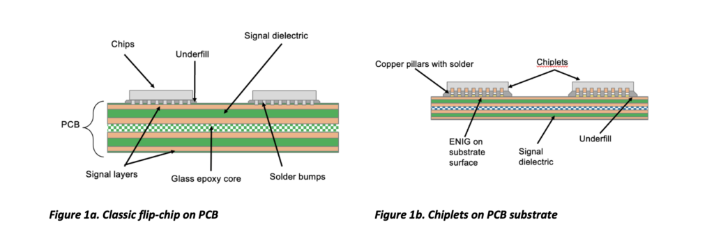
“Chiplet-last” describes a process by which the chiplet die are first bumped and then attached to a substrate or interposer. Flip-chipped onto a PCB is a common approach, as it is also often used with bare die. Figure 1a shows an example of a classic flip-chip on PCB uses a glass-epoxy core with only epoxy on the outer dielectric layers. Bumps are added to the die using conventional solder, and the die are underfilled to add mechanical strength.
A more advanced approach, shown in Figure 1b, is for two or more chiplets to be attached directly to a substrate. Substrate examples include an n-N-n PCB structure, glass-epoxy core, ABF build-up film interconnect dielectric, with ENIG (nickel + gold) on the substrate surface, with small (25-50µm) lines and spaces, and area of <100×100 mm. Copper pillars with ≤129µm pitch on the die are usually used. All of this taken together illustrates a step up in density for this approach.

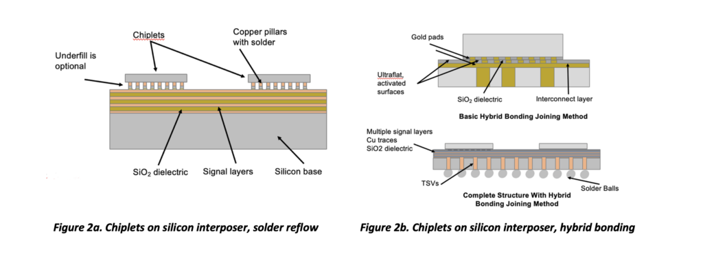
The next layer of sophistication for a chiplet-last approach is mounting the chiplet on a silicon interposer and then utilizing solder reflow (Figure 2a) to form the interconnects. With copper pillars you can use dielectric materials such as silicon oxide, polyimides or BT to build up a much higher-density interconnect structure. You can get down to 5 micron lines and spaces in an area of 35x35mm or less.
Hybrid bonding (Figure 2b) requires a very flat substrate with SiO2 and copper in the interconnect. The die is carefully placed and then bonded to the substrate using heat and pressure. This process enables fairly large, robust structures to be built, potentially using solder balls and through-silicon vias (TSVs) or by wire bonding from the top surface of the silicon interposer to a conventional PCB.

By contrast, the “chiplet-first” method is an RDL-like process. The chips are mounted with the active surfaces placed face-up, exposing the contact surfaces of all the chiplets and components well planarized. This process requires accurate location of connection points or an active patterning method to ensure connections are made to the chiplet contact area when die locations vary from site to site.
The interconnect is built with conductor and dielectric deposition and patterning steps, involving multiple copper interconnect layers, polyimide or epoxy dielectrics, and conductor-layer-to-conductor-layer microvias. For higher layers, lithographic masks can be used, but laser patterning can also suffice. Laser patterning is particularly useful when the pattern of the interconnect has to be modified from wafer to wafer due to small variations in die location.

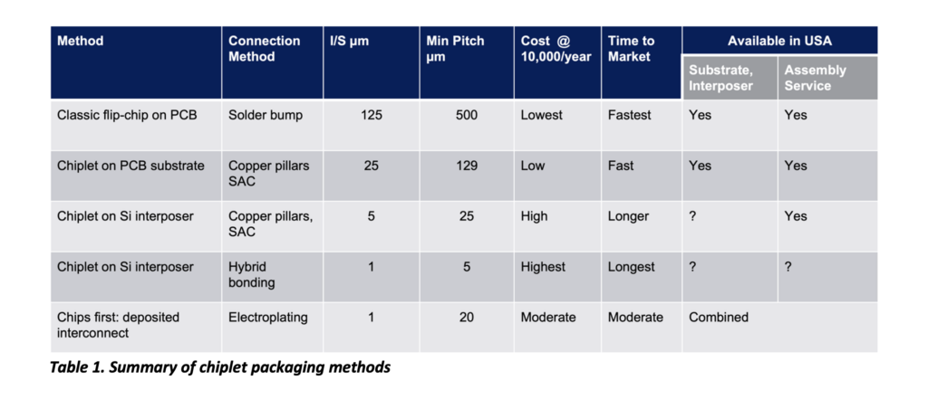
Table 1 summarizes the key features associated with each of the methods for optimizing chiplet packaging discussed above, along with cost and time-to-market parameters. Some are further along in development and implementation than others, but all require, or will require, capabilities such as those offered by QP Technologies.
As part of our proven assembly expertise, we offer a range of die bonding services essential to chiplet processes, including flip-chip, die attach, die-attach film (DAF), thermocompression, epoxy dispensing, and die stacking. Moreover, through our substrate development service, we can develop solutions leveraging advanced laminates such as FR-5, BT and ABF.
To learn more about our capabilities and get started on optimizing chiplet packaging, click here.

