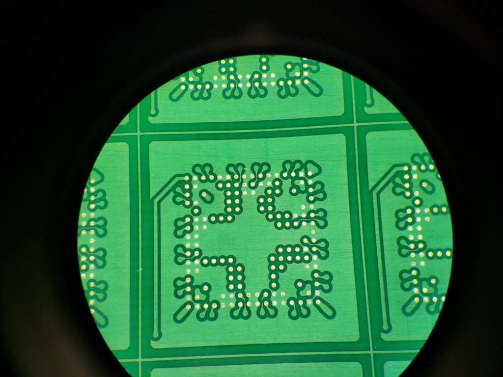
Substrate Development
We launched our substrate design, fabrication and assembly service to fill the gaps not met by standard, off-the-shelf packages. Through close collaboration, we create custom packaging solutions to your specifications. Using virtually any substrate type, we create turnkey solutions for substrate-based assemblies to meet your unique packaging requirements, with delivery times at least 50 percent faster than those of competitive services. We target both ICs and MEMS, and our ability to accommodate all types of substrates provides engineering flexibility that allows greater design freedom for a wide range of advanced packages.
One key driver for our substrate development service is the increased need for custom RF packages essential to 5G. Technologies in which we specialize, such as laminate quad flat no-lead (QFN) and organic QFN for flip-chips, are well suited to integration and customization. This is due to several factors, including small footprint, quick turn-time for leadframe redesign and fab, and low customization cost.
Demand for custom substrate packages is being driven by a number of other factors, as well:
- Growth of custom ICs
- Stringent speed, power and RF performance requirements (5G requires +40GHz frequencies)
- Inclusion of unique components with unique footprints
- Use of unique, non-square shapes
- Use of chip-scale packaging (CSP) to achieve smaller area and footprint, which is of particular value for medical, biotech and consumer applications
We can tune our process to optimize your desired parameter – size, performance, application – and create a solution in about five weeks, from initial consultation to finished assembly. Our service can also accommodate your needs for 3D packaging, ball grid arrays (BGAs), systems-in-package (SiPs), chiplets and multichip modules (MCMs). With this combination of quality, variety and speed, we continue broadening the reach of our service to address a range of markets, including military, medical, sensors and other custom arenas.

