Compound Semiconductors

Compound semiconductors are valued for their ability to support new circuit designs that help improve overall system performance and reduce costs. Primary compound technologies utilized for advanced device development include silicon carbide (SiC), gallium nitride (GaN), gallium arsenide (GaAs), graphene and indium phosphide (InP). SiC and GaN, in particular, have seen key gains in power, RF and photonics due to their wide-bandgap capabilities, which enable much faster speeds, higher power and smaller form factors than silicon-based chips.
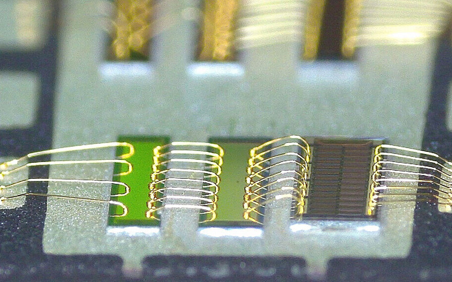
Packaging and assembly solutions that capitalize on these characteristics are essential to taking advantage of these capabilities while mitigating some of the challenges that packaging these devices present due to their unique physical properties. When working with GaN, for example, which operates in the 40-60GHz range, our engineers have worked to shorten wirebond lengths and loops using ribbon wirebonding, which is far more effective for these bandwidths.
QP Technologies has a wealth of demonstrated expertise in collaborating with our customers to formulate packaging solutions for compound semis, initiated with our design and engineering service. We consult with you to determine the right approach for your device, design and fabricate custom prototype packages to meet your specifications, and then complete the assembly process using your die. This encompasses a variety of materials and processes.
Our compound semiconductor capabilities include:
- Carrier Design & Fabrication (substrate, lead frame, metal tub)
Ceramic: DBC (ALN, AL2O3), BEO, ALN (THICK FILM), SI3N4, 3D Al2O3 with embedded cooling channels
Organic: Cores (FR4, Rogers, Arlon), stack-up technology
Lead frame: QFN (3×3 mm to 12X12 mm), custom lead frames (e.g., 64-lead TQFP-EP 10×10 mm)
OCPP: Remove old die and reuse package or substrate - Assemblies of Active devices (RF, digital, photonics, analog, mixed-signal)
GaN, GaAs, InP, SiGe, Silicon-on-Sapphire, SiC, graphene - Placement of Passive devices (caps, resistors, inductors)
Hardware (pins, connectors) - Final Package Manufacturing
System-in-Package (SiP): Combining various compound technologies into one final SiP
To download our white paper on the packaging solution leveraging compound semiconductor technology that we developed with Ideal Power for their B-TRAN™ bidirectional power switch devices, please click here. If you’re ready to engage with us on your compound semiconductor substrate project today, please click here.

