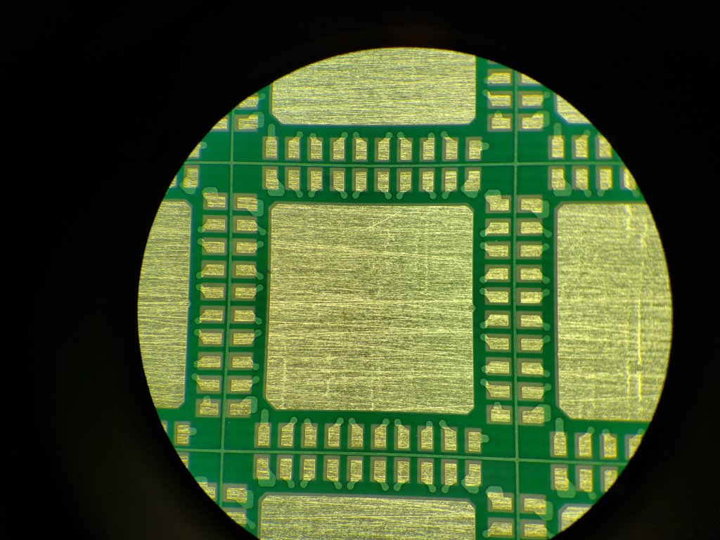
Substrate Design

As process node shrinks continue, substrate design becomes vital to successful product development. At these smaller nodes, the demand for higher-performance semiconductors in smaller packages is continuing to spur the development of advanced substrate materials that can support advancements in circuit design and fabrication.
As such, substrate design is not only integral to chip and package development – it may be the most critical factor in chip and system performance. Utilizing virtually any substrate type, QP Technologies (formerly Quik-Pak) can create turnkey solutions for substrate-based assemblies to accommodate your unique packaging requirements, with delivery times at least 50 percent faster than those of competitive services. We have designed some of the most advanced, high-performance substrates on the market for our industry-leading customers.
We can design substrates for a wide variety of packaging solutions, including:
- 2.5D/3D integration
- Flip chip or wirebond
- System in Package (SIP)
- Interposers
- RF devices
- MEMS
Our designers will ensure parts placement and critical routings meet both signal integrity and manufacturing requirements, following our design-for-manufacturing (DFM) rules, without sacrificing yield and cost considerations. If your product specifications include high-speed digital, high-density interconnect (HDI), analog/digital mix, high power, down-hole and/or radio frequency (RF) capabilities, our experienced team will work with you to develop the ultra-high-performance substrate that meets your needs.

