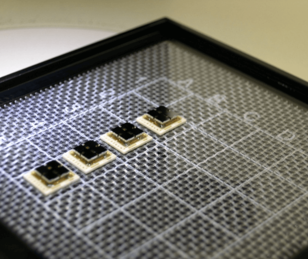
Flip Chip Bonding

Flip Chip assembly is the direct electrical connection of face-down (flipped) electronic die onto organic or ceramic circuit boards by means of conductive bumps on the chip bond pads. This process is quickly gaining popularity over traditional face-up wire bonding due to its advantages in circuit board real-estate reductions, performance, reliability, and cost over other packaging methods.
QP Technologies enhances bonding capabilities
QP Technologies (formerly Quik-Pak) has enhanced its Flip Chip bonding capability by installing a Finetech Pico Flip Chip bonder. The bonder is capable of placing pre-bumped devices within a 1µm placement accuracy. Assembly applications include µBGA, standard flip-chip, 3D packaging, optoelectronic bonding and assembly, sensors, chip on glass, and more.
QP Technologies Offers:
DEVICE BALL BUMPING:
- Solder ball bump to 305µm (0.012″) diameter on a 508µm (0.020″) pitch
- 96°C, 183°C, and 217°C alloys available
DEVICE/PARTIAL WAFER STUD BUMPING:
- Gold (Au) stud bumping of partial wafers and large die
- Stud bumping pitch down to 150µm
BONDING:
- Align down to 1µm placement accuracy
- Placement and bonding down to 100µm pitch devices
- Thermo-compression bonding of small gold-to-gold leads (highest accuracy)
- Thermosonic bonding of gold-to-gold leads (lower temperature)
- Hot air solder reflow for Sn, SnPb, and other solders
UNDERFILLS:
- Standard underfills for BGA and flip chip assemblies
- Reworkable underfills for BGA and flip chip assemblies where recovery of the substrate may be required

